Scientist at Forefront of US Army Research Selected to Lead PRC’s Strategic Chip Production Line
Scientist at Forefront of US Army Research Selected to Lead PRC’s Strategic Chip Production Line
Executive Summary:
- Beijing continues to exploit US policies to circumvent technology controls and to lower the scrutiny applied to its technology transfer activities.
- Hong Kong as part of the Greater Bay Area—is tasked to focus on third-generation chip production to leapfrog US and allied chokepoints in first-generation silicon chip production.
- The PRC’s ability to attract US-trained scientists and absorb research conducted at US institutions highlights grave concerns about US research security and the lack of regulations.
On July 30, the People’s Republic of China (PRC) announced the establishment of its third-generation chip production line in Hong Kong (HKCNA, July 30). This represents a significant move that underscores Beijing’s ambitions in the semiconductor industry. The new production line is spearheaded by renowned scientist Dr. Yitao Liao, who previously collaborated with the US Army on similar technologies. Both this new production line and Dr. Liao’s involvement raise questions about US policies toward the security and supervision of research into dual-use technology amid ongoing US-PRC rivalry.
Overview of the New Chip Production Line
The newly established chip production line is located in the Yuen Long Microelectronics Center (MEC) in Hong Kong, a facility set to be operational within this year. The project is driven by MassPhoton HK, a company founded by Dr. Yitao Liao. The primary focus of this initiative is the development of 8-inch Gallium Nitride (GaN) epitaxial wafers and the associated light emitting diode technology (LED) technology, which are essential for the advancement of third-generation semiconductor technologies (Mingpao, July 31; MassPhotonHK, last accessed August 5). The Chinese version of the company’s website mentions that they have established optical technology laboratories at Boston University in the United States—something left out of the English version.


The highlighted sentence on the company’s website mentions that they have a lab at Boston University, which is missing from the English version of the website. (Source: MassPhoton HK)
With an investment exceeding 200 million yuan ($27.9 million), the project aims to establish a pilot production line within three years, achieving an annual output of 10,000 GaN wafers. These wafers are crucial for applications in various high-tech fields, including electric vehicles, high-voltage power transmission, and artificial intelligence. Liao emphasized that the GaN epitaxial process is a key technology that can optimize product performance and enhance stability, making it a cornerstone of modern semiconductor advancements (Mingpao, July 31).
Significance of the Technology
In response to the US-PRC technology conflict, the PRC is strategically focusing on third-generation semiconductors to bypass US restrictions primarily targeting first-generation silicon-based semiconductors. Third-generation semiconductors, such as Gallium Nitride (GaN) epitaxial wafers, are alleged to have several advantages over traditional silicon-based chips. GaN wafers offer higher efficiency, faster switching speeds, and greater power handling capabilities, making them essential for applications in electric vehicles, green energy, and other high-tech fields. GaN technology also contributes to the development of high-performance LEDs, which are crucial for energy-efficient lighting. Advanced LEDs have played an increasing role in photonic chip manufacturing, which the PRC has been incrementally developing (IntechOpen, July 10, 2022; see China Brief, July 12). [1]
The 14th Five-Year Plan of Guangdong Province emphasizes the development of third-generation semiconductors, aiming to capture global market share and influence (Laoyaoba, May 4, 2021). According to Sun Dong, Hong Kong’s Secretary for Innovation, Technology, and Industry, Hong Kong has chosen as the site to develop this, as the city enjoys significantly reduced US restrictions on the importation of necessary manufacturing equipment for third-generation semiconductors (SCMP, July 30). He also mentions that this focus enables Hong Kong to align with the latest state policy of the Third Plenum, which supports making Hong Kong an international hub for high-end talent (HK01, July 30).
Dr. Yitao Liao: From US Collaborations to Chinese Leadership
Liao’s efforts support the PRC’s broader strategy of strengthening its semiconductor industry and transforming technologies for military purposes despite US restrictions. Liao’s involvement in this project adds another intriguing dimension to the story. Liao’s journey from the United States to the PRC is emblematic of broader trends in talent mobility, research security and technological transfer. Under the mentorship of Professor Theodore Moustakas, a pioneer in LED technology, Liao pursued his PhD research and later interned with an MIT company creating high-powered visible luminous devices for projection, which convinced him of the dual-use potential of LEDs (Boston University, February 10, 2017).
During his study at Boston University, Liao significantly advanced GaN and LED technology, particularly in developing high-efficiency deep ultraviolet (DUV) LEDs. His research includes enhancing Aluminum Gallium Nitride (AlGaN)-based DUV LEDs, improving their internal quantum efficiency for applications like disinfection and sterilization (AIP, February 21, 2011). [2] He has also explored the emission properties of GaN and the effects of band structure potential fluctuations to optimize LED performance (AIP, November 15, 2010). His contributions have been instrumental in expanding the practical and commercial viability of DUV-LED technologies.
The Photonics Center at Boston University has been collaborating with the US Army on photonic and LED technologies for years. Liao and his team played a central role in this research and received a grant from the US Army to develop UV LEDs to address US critical defense needs (Boston University, January 2012). Liao’s work with the US Army Research Laboratory focused on developing high-efficiency, high-power DUV-LEDs for various defense applications, including bacterial and viral detection, chemical and biological sensing, secure communication systems, non-destructive testing, and countermeasure systems (DTIC, May 6, 2015).
UV LEDs are highly desirable for a variety of consumer and industrial uses, such as medical devices for sterilization, water purification systems, and advanced lighting solutions (Boston University, February 10, 2017). Thus, the overlap between the defense-oriented research and commercial technology was evident. This would inspire Dr. Liao to found RayVio, a company devoted to commercializing his research into UV-LEDs. With the assistance of the Boston University Office of Technology Development (OTD), Liao filed patents and intellectual property licenses, and successfully connected with venture capitalists to fund his fledgling company (Boston University, February 10, 2017).
In 2020, Nitride Semiconductor, a Japanese UV-LED firm, won a patent infringement lawsuit against RayVio. The California Northern District federal court ruled that RayVio had infringed on Nitride’s patent, and the US Patent Office affirmed the validity of Nitride’s key claims. Consequently, RayVio was permanently closed, and its operations ceased (RayVio, accessed August 5).
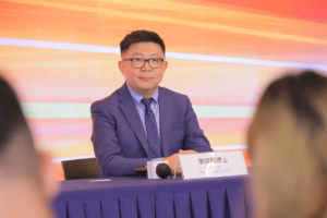
Dr. Yitao Liao attended the launch ceremony of third-generation semiconductor GaN epitaxial wafer pilot line in Hong Kong. (Source: HKSTP)
Liao’s peers, who had worked together previously on the US Army project, continue to play a key role in this field, as evidenced by the establishment of the Wide Bandgap Semiconductor Laboratory at Boston University (Wide Bandgap Semiconductor Laboratory, last accessed August 5; BU Photonics Center, last accessed August 5). As late as 2019, Liao filed the US patent “High Efficiency Ultraviolet Light Emitting Diode with Electron Tunneling”, which was published in 2023, and the assignee remains Boston University (USPTO, May 9, 2023).
In short, Liao’s longstanding research illustrates the critical role of GaN technology in advancing DUV-LED performance. His research underscores the dual-use nature of the technology and practical applications of GaN in both defense-related projects and commercial ventures, such as those previously pursued by RayVio and currently exemplified by the new chip production line in Hong Kong.
Conclusion
Dr. Yitao Liao’s journey from collaborating with the US military to leading the PRC’s new strategic chip production line in Hong Kong highlights the complex dynamics of talent mobility, technological transfer, and research security. His foundational work in developing high-efficiency, high-power deep ultraviolet LEDs not only demonstrated significant military potential but also paved the way for broader semiconductor applications.
Now, as Liao spearheads the establishment of a third-generation chip production line in Hong Kong—where the PRC has chosen to develop this technology—it is imperative for the United States to closely monitor these developments.
Protecting research security in the United States, particularly in the military and academia, requires understanding PRC strategies and operational patterns, especially concerning technologies that have dual civilian and military applications. The interactions between the two nations in technology and research can significantly shape the future landscape of innovation, competitiveness, and national security.
Notes
[1] While both GaN-based LEDs and UV lithography tools are forms of optical technology, they serve different purposes within the semiconductor industry. GaN-based LEDs are crucial for the development of photonic integrated circuits and advanced display technologies. On the other hand, advanced lithography tools such as EUV are essential for the precise patterning required in traditional silicon-based chip manufacturing.
[2] Quantum efficiency (QE) is the percentage of photons that a device can convert into electrons. This is used to measure the performance of photo-electronic devices in different applications, including solar cells, photodetectors (photodiodes, PD), avalanche photodiodes (APD), charge-coupled device (CCD) sensors, CMOS image sensors (CIS), and LEDs (Teledyne Princeton Instruments, accessed August 5; Enlitech, accessed August 5).